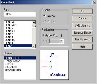
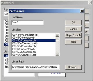
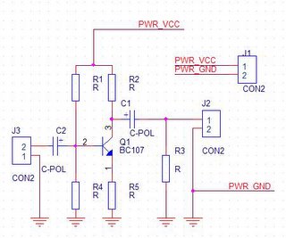
 Before we can manufacture a PCB, we need to know about the footprints and other related terms. Footprints are the pin layout of the components that you are using. For a circuit to be manufactured properly, its footprint must be properly selected. We select footprints for the components, in Capture CIS itself. But we will be using Layout to select footprints. Let?s start now.
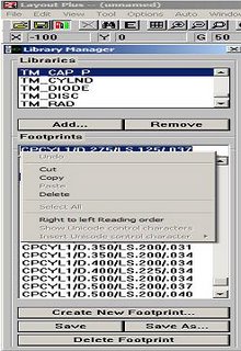
Start OrCAD Layout Plus from the programs menu. You may use OrCAD Layout or OrCAD Layout Engineer?s Edition in place of OrCAD Layout Plus. In Layout from the Tools menu, choose Library Manager. This will start a new window of Layout Plus with Library Manager loaded. Now find appropriate footprints for the components you use in circuit diagram. Some of the common libraries used for resistors and capacitors can be found in TM_AXIAL and TM_CAP_P sections. Similarly you can find footprints for other components if you explore the Library Manager a bit. Once you decide which footprint to use copy the name.
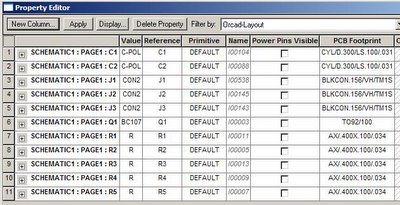
Still in OrCAD Capture CIS, press Control + A to select all the components and select Edit Properties. Now paste the footprint name in PCB Footprint column of the component you selected. After completing the above procedure for all components in the design, your Edit Properties window may look similar to one shown below. Once you complete all these steps then you can close Library Manager Window.
Now, its time to create a Netlist for our design. A netlist describes how different components in our design are interconnected and it also includes the PCB footprints. It is the input file for OrCAD Layout. We will create netlist in following steps.
- Select OrCAD Project workspace and select from Tools menu, Create Netlist option. A dialog box as shown below will appear. Use the settings shown.
- If the process completes without any errors, we can close OrCAD Capture CIS and start Layout Plus once again.
- In Layout Plus, from the File Menu, choose New and you will be asked for a Technology Template File, use default.tch and when asked for a file to save board give a name and location where you want to save the board.
- Now a new window with all components placed will be shown.
We will discuss Component Placing and routing in the next segment.

